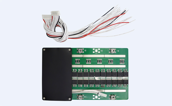
| Project | Symbol | The detailed content | NCM?Standard | LFP?Standard |
| Overcharge protection | VDET1 | Single overcharge detection voltage | 4.25V±0.03V | 3.65V±0.03V |
|
| tVDET1 | Overcharge detection delay time | 1.5s(MAX) | 1.5s(MAX) |
|
| VREL1 | Single overcharge release voltage | 4.15V±0.03V | 3.45V±0.03V |
|
| Cell balance | VBU | Cell-balance detection voltage | 4.2V±0.03V | 3.6V±0.03V |
|
| VBL | Cell-balance release voltage | 4.2V±0.04V | 3.59V±0.04V |
|
| IB | Balance current | 60mA±20mA | 60mA±20mA |
|
| Over-discharge protection | VDET2 | Single over-discharge detection voltage | 2.70V±0.1V | 2.50V±0.05V |
| tVDET2 | Overdischarge detection delay time | 1.5s(MAX) | 1.5s(MAX) |
| VREL2 | Single overdischarge release voltage | 3.0V±0.1V | 3.0V±0.05V |
|
| Over current protection | IDP1 | Level 1 overcurrent protection current | 150A±20A | 150A±30A |
| tVDET1 | Detection delay time | 1.0s(MAX) | 1.0s(MAX) |
| IDP2 | Level 2?overcurrent protection current | / | / |
| tVDET2 | Detection delay time | 300ms(MAX) | 300ms(MAX) |
| Short circuit protection | | Exterior short circuit | yes | yes |
|
| TSHORT | Detection delay time | 1500us(MAX) | 1500us(MAX) |
| Protection of release condition | Disconnecting the load | Disconnecting the load |
| Resistance | RDS | Main loop resistance (battery voltage = 3.4V) | B-至P- RDS≤20mΩ | B-至P- RDS≤20mΩ |
| Current consumption | IDD | Internal consumption during operation of the circuit | ≤60μA | ≤60μA |
| Charging maximum Voltage | VDS | Charging port connected to the charger maximum withstand voltage value | DC80V | DC80V |
| Chip maximum Voltage | VDS | Input voltage between each string battery node VDD-VSS | DC5V | DC5V |
| Continuous Discharge Current | | Sustainable discharge current | 50A | 150A |
| Continuous charge current |
| Sustainable charging current | 50A | 50A |
| Rated current temperature Mosfet | | Rated current discharge MOSFET surface temperature | <45° | <45° |
| Temperature control switch |
| Close the charging and discharging function at above rated temperature | Charging 75<℃ Discharging 75<℃ | Charging 75<℃ Discharging 75<℃ |
| Charging reverse protection | | When charging, avoid the positive polarity and negative polarity reversal of charging | NO | NO |
| PCB Size |
| PCB Length, Width, Thickness | ≦160*100*15mm | ≦160*100*15mm |